Energy Harvesting from Waste Heat and Sun Light with Mesoscopic Materials
 Tuesday June 18, 2013
Noon – 1 pm
Texas Instruments (TI) Auditorium E-1
2900 Semiconductor Drive
Santa Clara, CA
map
TITLE: Energy Harvesting from Waste Heat and Sun Light with Mesoscopic Materials
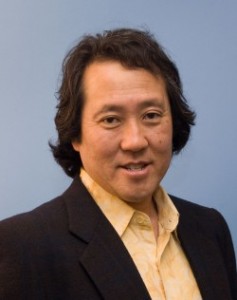
SPEAKER: Prof. Nobuhiko P. Kobayashi, Dept. of Electrical Engineering, UC Santa Cruz
ABSTRACT:
Designing solid-state devices is essentially restricted by choosing available chemical elements found on the Periodic Table and forming various stable solids made of these chemical elements. A key to developing novel solid-state devices is, therefore to find a route to combine a variety of such solids often physically and/or chemically incompatible each other to benefit from resulting combined material platforms. In this talk, specific examples of “Mesoscopic Materials” will be presented with the view toward solid-state devices for energy harvesting from waste heat and sun light. The talk is divided into the following two sections.
1. Semiconductor nanocomposites for energy harvesting from waste heat: thermoelectric.
2. Metal oxide thin films for high-power solar energy collection and transmission: Sun to fiber.
SPEAKER BIOGRAPHY:
Nobuhiko “Nobby” P. Kobayashi is a professor at the University of California Santa Cruz (UCSC) and the Science Director of Advanced Studies Laboratories, a strategic partnership between UCSC and NASA Ames Research Center. Current research projects include synthesis and characterization of nanometer-scale materials and devices with emphasis on solid-state energy conversion funded by DARPA, ONR, NSF, NASA, DOE, SRC, and ARPA-E. Prior to joining UCSC in 2008, Prof. Kobayashi was involved in developing electronic materials for memristive devices to build memories and logics required for future computing systems at Hewlett-Packard Laboratories. He also led semiconductor nanowire photonics for optical interconnect necessary for advanced computing systems. Prior to Hewlett-Packard Laboratories, Prof. Kobayashi worked at Lawrence Livermore National Laboratory, where he was involved in developing semiconductor materials for both ultra-high speed diagnosis systems required for the National Ignition Facility and the optical code division multiple access funded by DARPA. From 1999 to 2001, Prof. Kobayashi was at Agilent Laboratories, developing light emitting diodes, vertical cavity surface emitting lasers, and hetero bipolar transistors for ultra-wide band fiber-optics and high-speed wireless communications. Prof. Kobayashi earned his M.S. and Ph.D. degrees in materials science from University of Southern California in 1994 and 1998.
AGENDA:
- 11:30 am – Registration & light lunch (pizza & drinks)
- Noon – Presentation & Questions/Answers
- 1:00 pm – Adjourn
